Skip to main navigation menu
Skip to site footer
Home
Current
Archive
About the journal
Purpose and scope
Publication ethics
Preventing and combating plagiarism
Open access
Open data policy
Licensing
Archiving
Іndexing
Use of AI
Retraction policy
A brief history of the journal
Editorial board
For authors
Editorial process
Review process
Requirements for articles
Submissions
Article processing сharge
Journal copyright terms
Contacts
Search
Search
Register
Login
Home
/
Archives
/
No. 6 (2002): Tekhnologiya i konstruirovanie v elektronnoi apparature
ISSN 2225-5818 (Print)
ISSN 2309-9992 (Online)
Published:
2002-12-30

Full Issue
FULL ISSUE PDF (Українська)
Articles
Integrated approach to obtaining high-purity materials for microelectronics
V. M. Azhazha, G. P. Kovtun, I. M. Nekljudov
3-6
PDF (Українська)
Influence of fast neutron irradiation on epitaxial gallium arsenide
V. A. Zavadsky, S. V. Lenkov, D. V. Lukomsky, V. A. Mokritsky
7-9
PDF (Українська)
Mathematical modeling of degradation of ceramic thermistors with negative TCR
V. A. Balitskaya, N. M. Vakiv, O. I. Shpotyuk
10-13
PDF (Українська)
Methodology for determining the dynamic range of semiconductor photodetectors
I. V. Doktorovich, V. K. Butenko, V. N. Godovaniuk, V. G. Yurjev
14-15
PDF (Українська)
Spectral photosensitivity of Ni–Si:Au surface-barrier structures with injection amplification
Sh. D. Kurmashev, I. M. Vikulin, S. V. Lenkov, R. G. Sidorets
16-19
PDF (Українська)
Anisotropic thermoelectric comparator
A. A. Ashcheulov, I. V. Hutsul
20-21
PDF (Українська)
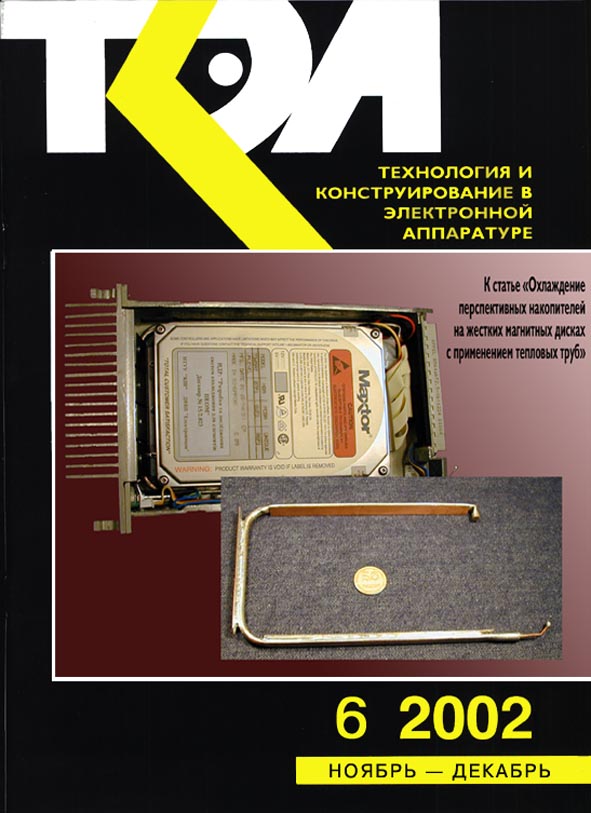
Cooling of promising hard disk drives using heat pipes
Yu. Ye. Nikolaienko, V. Yu. Kravets, V. A. Striuchenко, A. S. Belokonеnko
22-25
PDF (Українська)
Technological aspect of increasing the efficiency of semiconductor photovoltaic converters
V. V. Kurak, V. V. Tsybulenko, V. L. Agbomassou
26-29
PDF (Українська)
Complex doping of GaAs and InGaAs layers during liquid phase epitaxy
S. I. Krukovskyi
30-32
PDF (Українська)
Conditions for obtaining hollow silicon prisms for photovoltaic converters
B. P. Masenko
33-37
PDF (Українська)
Use of low-dimensional heterostructures of AIII-BV compounds in pressure sensors
I. Ye. Maronchuk, A. D. Kucheruk, S. Yu. Yerokhin, I. V. Chornyi
38-43
PDF (Українська)
Electrothermal element of gas sensors
Ya. I. Lepykh
43-44
PDF (Українська)
Modernization of the "Onyx" photonic annealing system for semiconductor wafers
H. V. Savytskyi, A. Yu. Bonchyk, I. I. Izhnin, S. H. Kyyak, I. A. Mohyliak, I. P. Trostinskyi
45-47
PDF (Українська)
Design and technological constraints in the design of high-voltage CMOS LSI circuits
V. H. Verbytskyi, V. I. Zolotarevskyi, Yu. Ye. Nikolaienko, L. I. Samotovka, E. S. Tovmach
48-53
PDF (Українська)
Contact-forming films of titanium borides and nitrides in gallium arsenide microwave devices
V. N. Ivanov, R. V. Konakova, V. V. Milenin, M. A. Stovpovoi
54-56
PDF (Українська)
Plasma technology for the formation of submicron LSI structures
S. P. Novosiadlyi
57-63
PDF (Українська)
Power microcircuit for control units of gas-discharge light sources
H. I. Havryliuk, V. V. Sevastianov, L. M. Bondarchuk, V. V. Chechel
63-64
PDF (Українська)
Archived version of TKEA website
Language
English
Українська
Information
For Readers
For Authors
For Librarians