Розробка математичної моделі фоточутливого сенсора Холла на основі CdS
Анотація
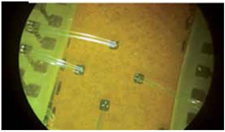
Запропоновано математичну модель фоточутливого сенсора Холла виготовленого на основі монокристала CdS, в якому використовується внутрішній фотоефект. Математична модель описує зміну концентрації та рухливості носіїв зарядів під дією опромінення й дозволяє оцінити приріст чутливості сенсора до магнітного поля завдяки зміні параметрів матеріалу сенсора. Теоретично встановлено і підтверджено експериментально, що при зовнішньому опроміненні активної області сенсора напруга Холла збільшується двократно. Розроблений підхід може бути використаний для оптимізації планарних сенсорів у системах, які потребують високої точності, чутливості та енергоефективності.
Посилання
S. M. Sze, Physics of Semiconductor Devices, 3rd ed. Hoboken, NJ, USA: Wiley, 2006.
M. J. Caruso, C. H. Smith, T. Bratland, and R. Schneider, “A new perspective on magnetic field sensing,” Sensors, vol. 17, no. 9, pp. 258–264, 2000. Available: https://surl.li/yyvpuk
W. Bolton, Sensors and Actuators: Engineering System Instrumentation, 2nd ed. Oxford, U.K.: Newnes, 2021.
L. Liu, X. Guo, W. Liu, and C. Lee, “Recent progress in the energy harvesting technology—From self-powered sensors to self-sustained IoT, and new applications,” Nanomaterials, vol. 11, no. 11, Art. no. 2975, 2021, doi: 10.3390/nano11112975.
A. Musiienko, R. Grill, P. Moravec, P. Fochuk, I. Vasylchenko, H. Elhadidy, et al., “Photo-Hall-effect spectroscopy with enhanced illumination in p-Cd1−xMnxTe showing negative differential photoconductivity,” Phys. Rev. Applied, vol. 10, pp. 014019, 2018, doi: 10.1103/PhysRevApplied.10.014019
S. E. Schacham, and E. Finkman, “Light-modulated Hall effect for extending characterization of semiconductor materials,” J. Appl. Phys., vol. 60, pp. 2860–2865, 1986, doi: 10.1063/1.337070
A. I. Galuza and A. B. Beznosov, “Optical functions of the Drude model: transformation of the spectra over wide ranges of parameters,” Low Temp. Phys., vol. 27, pp. 216–227, 2001, doi: 10.1063/1.1355519
N. J. Gantzler, “An alternative approach to the extended Drude model,” J. Appl. Spectrosc., vol. 85, pp. 361–364, 2018, doi: 10.1007/s10812-018-0657-x
I. V. Maznichenko, “Tunable 2D electron gas at the LaAlO3/SrTiO3(001) interface,” Phys. Rev. Materials, vol. 3, рр. 074006, 2019, doi: 10.1103/PhysRevMaterials.3.074006
J. H. Davies, “The two-dimensional electron gas,” in The Physics of Low-Dimensional Semiconductors: An Introduction, Cambridge: Cambridge University Press, 1997, pp. 329–370, doi: 10.1017/CBO9780511819070.011
P. Ritzinger, and K. Vyborny, “Anisotropic magnetoresistance: materials, models and applications,” R. Soc. Open Sci., vol. 10, iss. 10, 2023, doi: 10.1098/rsos.230564
C.-J. Zhao, “Research progress in anisotropic magnetoresistance,” Rare Metals, vol. 32, pp. 213–224, 2013, doi: 10.1007/s12598-013-0090-5
B. G. Streetman, and S. Banerjee, Solid State Electronic Devices, 6th ed. Upper Saddle River, NJ, USA: Prentice Hall, 2006.
V. Bruevich, H. H. Choi, and V. Podzorov, “The photo-Hall effect in high-mobility organic semiconductors,” Adv. Funct. Mater., vol. 31, pp. 2006178, 2021, doi: 10.1002/adfm.202006178
Y. Chen, H. T. Yi, and V. Podzorov, “High-resolution ac measurements of the Hall effect in organic field-effect transistors,” Phys. Rev. Applied, vol. 5, pp. 034008, 2016, doi: 10.1103/PhysRevApplied.5.034008
M. Schubert, P. Kühne, V. Darakchieva, and T. Hofmann, “Optical Hall effect model description: tutorial,” J. Opt. Soc. Am. A, vol. 33, pp. 1553–1568, 2016, doi: 10.1364/JOSAA.33.001553
C. Jacoboni, and L. Reggiani, “The Monte Carlo method for the solution of charge transport in semiconductors with applications to covalent materials,” Rev. Mod. Phys., vol. 55, no. 3, pp. 645–705, 1983, doi: 10.1103/RevModPhys.55.645
Y. Tsividis, and C. McAndrew, Operation and Modeling of the MOS Transistor, 3rd ed. Oxford, U.K.: Oxford Univ. Press, 2011.
R. S. Popovic, Hall Effect Devices: Magnetic Sensors and Characterization of Semiconductors. Bristol, U.K.: Institute of Physics Publishing, 2004.
R. F. Pierret, Semiconductor Device Fundamentals. Reading, MA, USA: Addison Wesley, 1996.
M. Razeghi, and R. Baker, Modern Semiconductor Device Physics. San Diego, CA, USA: Academic Press, 2007.
J. Singh, Semiconductor Optoelectronics: Physics and Technology. New York, NY, USA: McGraw-Hill, 2003.
P. Y. Yu, and M. Cardona, Fundamentals of Semiconductors: Physics and Materials Properties, 4th ed. Berlin, Germany: Springer, 2010, doi: 10.1007/978-3-642-00710-1
J. I. Pankove, Optical Processes in Semiconductors. New York, NY, USA: Dover Publications, 1971.
D. K. Ferry, and S. M. Goodnick, Transport in Nanostructures. Cambridge, U.K.: Cambridge Univ. Press, 1997, doi: 10.1017/CBO9780511626128
R. A. Smith. Semiconductor Fundamentals. Oxford University Press, 2014.
B. Ch. Burgett, and C. Ch. Lin, “Infrared quenching of the luminescence and photo-hall effect of ZnS:Cu and CdS:Cu crystals”, Journal of Physics and Chemistry of Solids, vol. 31, iss. 6, 1970, pp. 1353–1359, doi: 10.1016/0022-3697(70)90139-3.
J. H. Davies, The Physics of Low-Dimensional Semiconductors: An Introduction. Cambridge University Press, 1998.
B. K. Ridley, Quantum Processes in Semiconductors (5th ed.). Oxford University Press, 2013.
Авторське право (c) 2025 Віктор Сергійчук, Остап Олійник

Ця робота ліцензується відповідно до Creative Commons Attribution 4.0 International License.
