Деформаційно-стимульовані ефекти в мікроструктурах антимоніду індію за кріогенних температур для сенсорних застосувань
Анотація
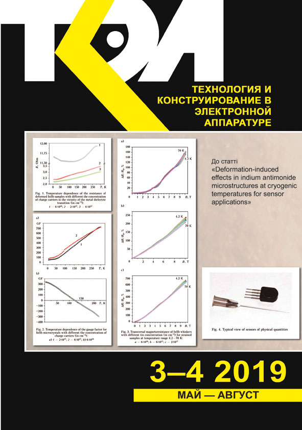
У роботі досліджено деформаційно-стимульоване змінення електрофізичних параметрів ниткоподібних кристалів антимоніду індію за кріогенних температур у сильних магнітних полях (до 10 Тл). Ниткоподібні кристалі InSb вирощувалися методом хімічних газотранспортних реакцій. Температура зони кристалізації становила 720 К, зони випаровування — 850 К. Легування кристалів здійснювалося домішкою олова в процесі росту, а концентрація носіїв заряду, згідно з дослідженнями Холла, становила 6·1016 — 6·1017 см–3. Для досліджень були вибрані ниткоподібні кристали InSb довжиною 2—3 мм з поперечними розмірами близько 30—40 мкм. Електричні контакти до ниткоподібних кристалів InSb були створені за допомогою мікродротів Au діаметром 10 мкм, які утворюють евтектику з мікрокристалом під час імпульсного зварювання.
Електропровідність ниткоподібних кристалів InSb досліджувалася в діапазоні температури від 4,2 до 300 К. Кристали охолоджували в гелієвому кріостаті. Температуру вимірювали за допомогою термопари Cu–CuFe, каліброваної за допомогою сенсора CERNOX. Деформацію зразків (ε = –3·10–4 відн. од. при 4,2 К) створювали за рахунок різниці в коефіцієнтах термічного розширення ниткоподібних кристалів та матеріалу підкладки, закріплюючи кристали на мідній підкладці та охолоджуючи до низьких температур.
На основі порівняння опору деформованих та недеформованих кристалів були визначені коефіцієнти тензочутливості. Значення коефіцієнта тензочутливості мікрокристалів InSb за температури рідкого гелію становить GF4.2K ≈ 72 за концентрації носіїв заряду 2·1017 см–3 та GF4.2K ≈ 47 за концентрації 6·1017 см–3. Для зразків InSb з концентрацією 6·1016 см–3 коефіцієнт тензочутливості виявляє нетипові властивості: вище температури рідкого азоту він змінює свій знак з позитивного на негативний. Абсолютне значення коефіцієнта тензочутливості як за гелієвих температур, так і в області кімнатної досягає приблизно 350, що можна пояснити наближенням концентрації носіїв заряду до фазового переходу «метал — діелектрик».
Встановлено, що для застосування в п'єзорезистивних датчиках, працездатних в широкому температурному діапазоні (4,2—300 К), слід використовувати мікрокристали InSb з концентрацією носіїв заряду 6·1016 см–3. Для розробки датчиків магнітного поля з магніторезистивним принципом дії використовується ефект гігантського магнетоопору, який досягає 720% за температури 4,2 К. Такий датчик містить деформовані мікрокристали InSb з концентрацією носіїв заряду, що відповідає металевому боку переходу «метал — діелектрик» і становить 2·1017 см–3. Розроблений мікроелектронний датчик має надвисоку чутливість до магнітного поля (1500 мВ/Тл), а простота конструкції забезпечує одночасно низьку інерційність та високу продуктивність.
Посилання
Zutic I., Fabian Ja., Das Sarma S. Spintronics: Fundamentals and applications. Rev. Mod. Phys., 2004, vol. 76, iss. 2, 323. https://doi.org/10.1103/RevModPhys.76.323
Holota V.I., Kogut I., Druzhinin A., Khoverko Y. High sensitive active MOS photodetector on the local 3D SOI-structure. Advanced Materials Research, 2014, vol. 854, pp. 45–47. https://doi.org/10.4028/www.scientific.net/AMR.854.45
Druzhinin A., Ostrovskii I., Khoverko Yu., LiakhKaguy N. Negative magnetoresistance in indium antimonide whiskers doped with tin. Low Temperature Physics, 2016, vol. 42, pp. 453–457. https://doi.org/10.1063/1.4954778
Nepijko S.A., Kutnyakhov D., Odnodvorets L.V., Protsenko S.I. Sensor and microelectronic elements based on nanoscale granular systems. J. Nanopart. Res., 2011, vol. 13, iss. 12, p. 6263–6281. https://doi.org/10.1007/s11051-011-0560-3
Mangin S., Ravelosona D., Katine J.A. et al. Currentinduced magnetization reversal in nanopillars with perpendicular anisotropy. Nat. Mater., 2006, no. 5, pp. 210–215. https://doi.org/10.1038/nmat1595
Berger L. Emission of spin waves by a magnetic multilayer traversed by a current. Phys. Rev. B, 1996, vol. 54, iss. 13, 9353. https://doi.org/10.1103/PhysRevB.54.9353
Slonczewski J.C. Current-driven excitation of magnetic multilayers. J. Magn. Magn. Mater., 1996, vol. 159, iss. 1–2, L1–L7. https://doi.org/10.1016/0304-8853(96)00062-5
Waintal X., Myers E.B., Brouwer P.W., Ralph D.C. Role of spin-dependent interface scattering in generating current-induced torques in magnetic multilayers. Phys. Rev. B, 2000, vol. 62, iss. 18, 12317. https://doi.org/10.1103/PhysRevB.62.12317
Stiles M.D., Zangwill A. Anatomy of spin-transfer torque. Phys. Rev. B, 2002, vol. 66, iss. 1, 014407. https://doi.org/10.1103/PhysRevB.66.014407
Volkov S.О., Tkach О.P., Odnodvorets L.V., Huzhnya Ya.V. Magnetoresistive properties of nanosized film materials: variation of measuring currents and minimization of electronic noise. Journal Nano- And Electronic Physics, 2016, vol. 8, iss. 3, 0303. http://dx.doi.org/10.21272/jnep.8(3).03030
Druzhinin A., Ostrovskii I., Khoverko Yu., Yatsukhnenko S. Magnetic properties of doped Si whiskers for spintronics. Journal of Nano Research, 2016, vol. 39, pp. 43–54. https://doi.org/10.4028/www.scientific.net/JNanoR.39.43
Yatsukhnenko S., Druzhinin A., Ostrovskii I. et al. Nanoscale conductive channels in silicon whiskers with nickel impurity. Nanoscale Research Letters, 2017, vol. 12, iss. 78, pp. 1–7. https://doi.org/10.1186/s11671-017-1855-9
Druzhinin A., Ostrovskii I., Khoverko Y. et al. Peculiarities of magnetoresistance in InSb whiskers at cryogenic temperatures. Materials Research Bulletin, 2015, vol. 72, pp. 324–330. https://doi.org/10.1016/j.materresbull.2015.08.016
Druzhinin A., Ostrovskii I., Khoverko Yu. et al. Berry phase in strained InSb whiskers. Low Temperature Physics, 2018, vol. 44, pp. 1189–1194. https://doi.org/10.1063/1.5060974
Murakawa H., Bahramy M. S., Tokunaga M. et al. Detection of Berry’s phase in a bulk Rashba semiconductor. Science, 2013, vol. 342, iss. 6165, pp. 1490–1493. https://doi.org/10.1126/science.1242247
Veldhorst M ., Snelder M ., Hoek M . et al . Magnetotransport and induced superconductivity in Bi based three-dimensional topological insulators. Phys. Status Solidi, 2013, vol. 7, iss. 1–2, pp. 26–38. https://doi.org/10.1002/pssr.201206408
Nikolaeva A., Konopko L., Huberc T. E. et al. Effect of weak and high magnetic fields in longitudinal and transverse configurations on maneto-thermoelectric properties of quantum Bi wires. Surface Engineering and Applied Electrochemistry, 2014, vol. 50, iss. 1, pp. 57–62. http://dx.doi.org/10.3103/S1068375514010128
Druzhinin A.A., Lavitska E.N., Maryamova I.I., Kunert H.W. Stress imposing during microcrystals characterization at cryogenic temperatures. Advanced Engineering Materials, 2002, vol. 4, iss. 8, pp. 589–592. https://doi.org/10.1002/1527-648(20020806)4:8%3C589::AIDADEM589%3E3.0.CO;2-F
Xiaoling Zhang, Qingduan Meng, Liwen Zhang. Dependence of the deformation of 128×128 InSb focalplane arrays on the silicon readout integrated circuit thickness. The Open Electrical & Electronic Engineering Journal, 2015, vol. 9, pp. 170–174. http://dx.doi.org/10.2174/1874129001509010170
Liwen Zhang, Jiexin Pu1, Ming Shao, Na Li. Numerical simulation and analysis of thermal stress in 8×8 InSb detector integrated microlens arrays with underfill. Journal of Convergence Information Technology, 2012, vol. 7, iss. 8.
Botcharova E., Freudenberger J., Schultz L. Mechanical and electrical properties of mechanically alloyed nanocrystalline Cu–Nb alloys. Acta Materialia, 2006, vol. 54, iss. 12, pp. 3333–3341. https://doi.org/10.1016/j.actamat.2006.03.021
Smith C.S. Piezoresistance effect in germanium and silicon. Phys. Rev., 1954, vol. 94, iss. 1, pp. 42–49. https://doi.org/10.1103/PhysRev.94.42
Druzhinin A., Ostrovskii I., Khoverko Yu. et al. Variable-range hopping conductance in Si whiskers. Phys. Status Solidi A, 2014, vol. 211, iss. 2, pp. 504–508. https://doi.org/10.1002/pssa.201300162
Vanger А .I . , Zabrodsk i i А .G . , T isnek Т .V . Magnetoresistance of compensated Ge:As at ultrahigh frequencies in the metal-insulator phase transition region. FTP, 2000, vol. 34, iss. 7, pp. 774–782. (Rus). https://journals.ioffe.ru/articles/37181
Litvinenko K.L., Nikzad L., Pidgeon C.R. et al. Temperature dependence of the electron Landé g factor in InSb and GaAs. Phys. Rev. B, 2008, vol. 77, iss. 3, 033204. https://doi.org/10.1103/PhysRevB.77.033204
Barlian A.A., Park S.J., Mukundan V., Pruitt B.L. Design and characterization of microfabricated piezoresistive floating element-based shear stress sensors. Sens. Actuators A, 2007, vol. 134, iss. 1, pp. 77–87. https://doi.org/10.1016/j.sna.2006.04.035
Naumova O.V., Popov V.P., Aseev A.I. et al. Siliconon-insulator nanowire transistor for medical biosensors. In EuroSOI International conference, 2009, Goteborg, pp. 69–70. https://doi.org/10.1007/978-3-642-15868-1
Günel H. Y., Batov I. E., Hardtdegen H. et al. Supercurrent in Nb/InAs-nanowire/Nb Josephson junctions. J. Appl. Phys., 2012, vol. 112, iss. 3, 034316. https://doi.org/10.1063/1.4745024
Claeys C., Simon E. Perspectives of silicon-oninsulator technologies for cryogenic electronics. In: Hemment P.L.F., Lysenko V.S., Nazarov A.N. (eds) Perspectives, Science and Technologies for Novel Silicon on Insulator Devices. NATO Science Series (Series 3. High Technology), vol. 73. Springer, Dordrecht. https://doi.org/10.1007/978-94-011-4261-8_23
Rife J.C., Miller M.M., Sheehan P.E. et al. Design and performance of GMR sensors for the detection of magnetic microbeads in biosensors. Sensors and Actuators, 2003, A107, pp. 209–218. https://doi.org/10.1016/S0924-4247(03)00380-7
Lagae L., Wirix-Speetjens R., Das J. et al. On-chip manipulation and magnetization assessment of magnetic bead ensembles by integrated spin-valve sensors. J. Appl. Phys., 2002, vol. 91, iss. 7786, pp. 7445–7447. https://doi.org/10.1063/1.1447288
Авторське право (c) 2019 Дружинін А. О., Ховерко Ю. М., Островський І. П., Лях-Кагуй Н. С., Пасинкова О. А.

Ця робота ліцензується відповідно до Creative Commons Attribution 4.0 International License.
