Indium antimonide nanowires arrays for promising thermoelectric converters
Abstract
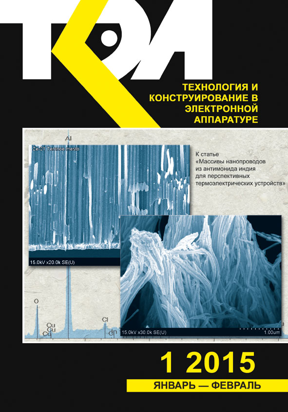
The authors have theoretically substantiated the possibility to create promising thermoelectric converters based on quantum wires. The calculations have shown that the use of quantum wires with lateral dimensions smaller than quantum confinement values and high concentration and mobility of electrons, can lead to a substantial cooling of one of the contacts up to tens of degrees and to the heating of the other. The technological methods of manufacturing of indium antimonide nanowires arrays with high aspect ratio of the nanowire diameters to their length in the modified nanoporous anodic alumina matrixes were developed and tested. The microstructure and composition of the formed nanostructures were investigated. The electron microscopy allowed establishing that within each pore nanowires are formed with diameters of 35 nm and a length of 35 microns (equal to the matrix thickness). The electron probe x-ray microanalysis has shown that the atomic ratio of indium and antimony in the semiconductor nanostructures amounted to 38.26% and 61.74%, respectively. The current-voltage measurement between the upper and lower contacts of Cu/InSb/Cu structure (1 mm2) has shown that at 2.82 V negative voltage at the emitter contact, current density is 129.8 A/cм2, and the collector contact is heated up to 75 degrees during 150 sec. Thus, the experimental results confirmed the theoretical findings that the quantum wire systems can be used to create thermoelectric devices, which can be widely applied in electronics, in particular, for cooling integrated circuits (processors), thermal controlling of the electrical circuits by changing voltage value.
References
Landis S. Nano-lithography, London UK: ISTE, Hoboken NJ: Wiley, 2011, 345 p.
Demikhovskii V. Ya., Vugal’ter G. A. Fizika kvantovykh nizkorazmernykh struktur [Physics of the quantum low-dimensional structures]. Moscow, Logos, 2000, 248 p. (Rus)
Obukhov I. A. Selfcooling of the quantum wire’s emitter contact. Journal of nano and Microsystem Technique, 2007, vol. 5, pp. 21-23. (Rus)
Obukhov I. A. Influence of external electromagnetic radiation on current voltage characteristics of quantun wire. 20th Int. Crimean Conf. “Microwave & Telecommunication Technology”, Ukraine, Sevastopol, 2010, pp. 833-835. (Rus)
Obukhov I. A. Nonequilibrium effects in one-dimensional quantum devices, Lambert Academic Publishing, 2014, 132 p.
Khan M. I., Penchev M., Jing X. et al. Electrochemical growth of InSb nanowires and report of a single nanowire field effect transistor. Journal of Nanoelectronics and Optoelectronics, 2008, vol. 3, no 2, pp. 199-202. http://dx.doi.org/10.1166/jno.2008.203
Chen H., Sun X., Lai K. W. C., Meyyappan M., Xi N. Infrared detection using an InSb nanowire. Proceed. Of IEEE Nanotechnology Materials and Devices Conference (NMDC’09), USA, Traverse City, 2009, pp. 212-216.
Obuhov I. A. Neravnovesnye effekty v elektronnykh priborakh [Non-equilibrium effects in electronic devices]. Sevastopol’, Veber, 2010, 303 p. (Rus)
Yang X., Wang G., Slattery P. et al. Ultrasmall single-crystal indium antimonide nanowires. Crystal Growth and Design, 2010, vol. 10, iss. 10, pp. 2479-2482. http://dx.doi.org/10.1021/cg100376u
Vasil’ev R. B., Dirin D. N. Kvantovye tochki: sintez, svoistva, primenenie [Quantum dots: synthesis, properties and applications]. Moscow, FNM, 2007, 34 p. (Rus)
Khan M. I., Wang X., Bozhilov K. N., Ozkan C. S. Templated fabrication of InSb nanowires for nanoelectronics. Journal of Nanomaterials, 2008, vol. 2008, pp. 1-5. http://dx.doi.org/10.1155/2008/698759
Gorokh G. G, Obukhov I. A., Lozovenko A. A. et al. Template method of forming InSb large aspect ratio quantum nanowires. 23rd Int. Crimean Conf. “Microwave & Telecommunication Technology”, Ukraine, Sevastopol, 2013, рр . 820-823. (Rus)
Gorokh G. G., Obukhov I. A., Poznyak A. A. et al. Synthesis of InSb nanowires in anodic alumina modified matrixes // 22nd Int. Crimean Conf. “Microwave & Telecommunication Technology”, Ukraine, Sevastopol, 2012, рр. 655-658. (Rus)
Gorokh G., Obukhov I., Lozovenko A. et al. [Formation of InSb nanowires in porous anodic alumina]. Proceed. VII International Conference “Fullerenes and nanostructures in condensed matter”, 2013, pp. 377-387. (Rus)
Obukhov I. A. Modelirovanie perenosa zaryada v mezoskopicheskikh strukturakh [Simulation of charge transport in mesoscopic structures]. Sevastopol, Veber, 2005, 226 p. (Rus)
Obukhov I. A., Gorokh G. G. [InSb-based electron devices]. 22nd Int. Crimean Conf. “Microwave & Telecommunication Technology”, Ukraine, Sevastopol, 2012, pp. 653-654. (Rus)
Wood G. C. Oxides and oxide films. USA, New York, Marcell Dekker, 1987, 537 p.
Ganzha S.V., Kukhareva N.V., Grushevskayа S.N., Vvedenskii A.V. [The kinetics of the formation of Cu(I) and Cu(II) oxides on copper in alkaline solutions and the features of their photoelectrochemical behavior. Part II. Photopotential]. Condensed matter and interphase boundaries, 2010, pp. 42-52. (Rus)
Ganzha S.V., Maksimova S.N., Grushevskaya S.N., Vvedenskii A.V. Formation of oxides on copper in alkaline solution and their photoelectrochemical properties. Protection of Metals and Physical Chemistry of Surfaces, 2011, vol. 47, no 2, pp. 191-202.
Grushevskayа S.N., Eliseev D. S., Ganzha S.V., Vvedenskii A.V. [The Properties of Semiconducting Copper Oxides Formed on Cu-Au Alloys]. Condensed matter and interphase boundaries, 2013, vol/ 15, no 3, pp. 253-265. (Rus)
Obuhov I. A. [Features of functioning of quantum devices]. Journal of nano and Microsystem Technique, 2009, no 7, pp. 38-45. (Rus)
Copyright (c) 2015 Gorokh G. G., Obukhov I. A., Lozovenko A. A.

This work is licensed under a Creative Commons Attribution 4.0 International License.
