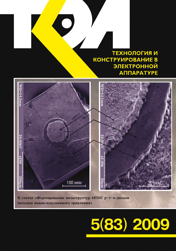
Forming of 4НSiC p–i–n-diodes mesastructures by the ion-plasmous etching method
Keywords:
p–i–n-diode, 4NSiC silicon carbide, ion-plasma etching, silicon etching, mesastructure, diode chip
Abstract
The results of research and optimization of 4НSiC p–i–n-diodes mesastructures manufacturing method are presented, as well as analysis of current-voltage characteristics and switching characteristics of p–i–n-diodes in the 25—500°C temperature range.
Published
2009-10-30
How to Cite
Boltovets, M. S., Borisenko, A. G., Ivanov, V. N., FedorovichО. А., Krivutsa, V. A., & Polozov, B. P. (2009). Forming of 4НSiC p–i–n-diodes mesastructures by the ion-plasmous etching method. Technology and Design in Electronic Equipment, (5), 45-48. Retrieved from https://www.tkea.com.ua/index.php/journal/article/view/TKEA2009.5.45
Section
Articles
Copyright (c) 2009 Boltovets M. S., Borisenko A. G., Ivanov V. N., Fedorovich О. А., Krivutsa V. A., Polozov B. P.

This work is licensed under a Creative Commons Attribution 4.0 International License.
